Electron Microscope of Tomorrow: Automation Meets Data Analytics
Electron microscopy and instrumentation in scientific discovery
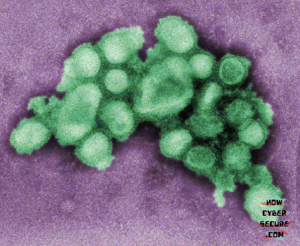
This article focuses on the role of electron microscopy in scientific practice and innovation in many different fields, such as biology, chemistry, physics, ecology and engineering. In this view the paper considers microscopes and how they can become an instrument of discovery; it provides a review of the different types of microscopy: scanning electron microscopy (SEM) and transmission electron microscopy (TEM). The analysis focuses on the instruments that have been successfully used for scientific purposes, such as the electron microscope and the scanning micro-imaging systems (SMLIS). It is shown that a wide range of different microscopy forms can provide information about biological phenomena. In addition, a special attention is paid to the new generation of electron microscopes that are capable of imaging in three dimensions (3D) in addition to in 2D at high resolution. The 3D imaging capabilities are obtained thanks to the use of very high-precision electron detectors that use a spatial collimation scheme. This chapter also covers the technologies used in the 3D microscopy systems. It describes how these systems can be used in life science, in the field of chemistry and physics, for the direct monitoring of new materials and processes, and for high-resolution nanoscopy. It also considers the use of various software and applications that enable scientists to visualize the results obtained with the instruments. In general it is stated that the use of electron microscopy has greatly contributed to the growth of science and technology based on the image of the world; it has been a decisive instrument for the creation of new scientific theories and for the advancement of scientific knowledge.

The Electron Microscope of Tomorrow: Automation meets Data Analytics
The Electron Microscope of Tomorrow: Automation meets Data Analytics. Computer Hardware.
The future of a field, especially one as technical as semiconductor manufacturing, is becoming increasingly dependent on automated systems. This issue of Computer Hardware highlights a recent effort to automate the microscopic inspection of semiconductor wafers through a machine vision system. The article discusses the progress that was made in the design and development of the machine vision system as well as the results obtained from the experiment.
The process of manufacturing a device or a system by utilizing semiconductor elements has been a long and complex one. This article briefly summarizes the history of this process.
A key component of a semiconductor device is a substrate on which a semiconductor element is to be fabricated. On the substrate, semiconductor elements are fabricated by forming semiconductor thin films, which are referred to as semiconductor layers, over a surface of a semiconductor substrate. The semiconductor elements are then patterned for the purpose of forming desired electrical circuit elements in the semiconductor element.
Today’s semiconductor devices are made through a series of many steps. For one of these steps, various types of processing are carried out on a semiconductor substrate to provide an integrated circuit. Such processing may be performed by etching of the substrate, etching of layers of material grown on the substrate, chemical vapor deposition of materials, epitaxial growth of layers, and the like. Such step, however, is usually carried out in a vacuum. Therefore, semiconductor elements formed of single crystal substrates or wafers are not fabricated in the vacuum environment. Instead, semiconductor elements fabricated by a process called a “lithography process” in which an image of the desired pattern is transferred to a pattern on a mask, is fabricated in the vacuum environment.
A lithography process may be carried out in a high-temperature, high-pressure environment in a processing chamber filled with ultra-high-vacuum.

Microscopy & Microanalysis : status and perspectives
Microscopy is used to probe and analyze objects and surfaces. In the biological sciences, this can be accomplished in a wide array of ways, including light, electron, or ion microscopy. The latter two are used in conjunction with various techniques to generate high-resolution images (i. , 3D) and high-flux or fluorescent detection. The two common methods for capturing images on a microscope are confocal and structured illumination. Confocal microscopy works by collecting a series of optical sections through a stack of samples and is generally useful for obtaining images of subcellular structures. For this, the specimen is stained with a specific marker and the images are obtained by imaging each cell or vesicle separately. Structured illumination produces high-resolution images by illuminating the specimen with a beam that is focused on each pixel of the image and then by diffusing the illuminating beam through each pixel. This technique is often useful for imaging the surface of a sample, like the surface of an organism, where the amount of information to be contained in a single image is quite limited due to the relatively small number of surface points.
Microscopy is a microscopic operation that can be used to observe objects or surfaces. Microscopes are commonly used for microscopy of biological specimens, but can also be applied to imaging structures of other materials at greater resolution.
Microscopy is a powerful analytical and imaging technology, but it has many applications outside the biological sciences. For instance, it can be applied to many engineering fields where images and 3D models cannot easily be obtained. Other uses of microscopy include the construction of structures at nanoscale resolution that are not accessible by any other means, imaging of biological processes, analyzing nanoscale defects or other features on a surface or for the construction of 3D models, and other applications are numerous.
Microscopes are designed for many applications, but they have other specialized use, such as for image-based cytology or for medical imaging.
Microscopy is the combination, observation, and interpretation of light and dark to obtain high-resolution images of objects and surfaces. Different microscopes have different capabilities and specifications.
Tips of the Day in Computer Hardware
The hardware we use every day is complex, changing with time and the needs of our applications, and the hardware market is constantly evolving. Today we will dive into the design and design of some of the critical hardware components that we use everyday, as well as some that we have used in the past.
The computer is the heart of every modern office productivity suite. It can be configured at different speeds; from medium-fast, slow, high-speed, standard, and super-fast to the faster of medium-faster, medium-slow, and super-slow. It is a key component in the design of most office productivity suites.
The computer and peripherals are the most expensive component in a modern office productivity suite (see Figure 1). This is due to the fact that the computer, the motherboard, the processor, the disk drive, and the memory modules, are all important functional components. Each of these components is more expensive than its predecessor in order to maintain quality (in manufacturing, in performance, at the lowest prices).
Related Posts:


Spread the loveElectron microscopy and instrumentation in scientific discovery This article focuses on the role of electron microscopy in scientific practice and innovation in many different fields, such as biology, chemistry, physics, ecology and engineering. In this view the paper considers microscopes and how they can become an instrument of discovery; it provides a review…